Electronics Design
Table of content:
1 - Individual assignment1.1 - Degign 1.2 - Milling 1.3 - Soldering 1.4 - Programming
2 - Group assignment
Individual assignment
The individual assignment was to re-draw the hello world board by adding at least one led and one button and program it to check whether the board is in working condition or not.
Design
For designing the pcb, i used autodesk’s eagle. I still don’t know a lot about the software so i’ll mention the things that i know and what i
did for designing the pcb
<<<---SAVE THE SCHEMATIC--->>>
After opening the software, the first thing to do is create a schematic file. File > new > schematic. A new schematic window will open. It is
always recommended to save the file first before starting working on the schematic.
<<<---ADD THE COMPONENTS--->>>
Add the components you need to make the PCB. You can add them from the libraries that are pre-installed in the software and you can also add
your own library containing all the components. You can select the “add part” from the left panel as well as search the “add part” command
from the search bar. You can select all the feature using same method
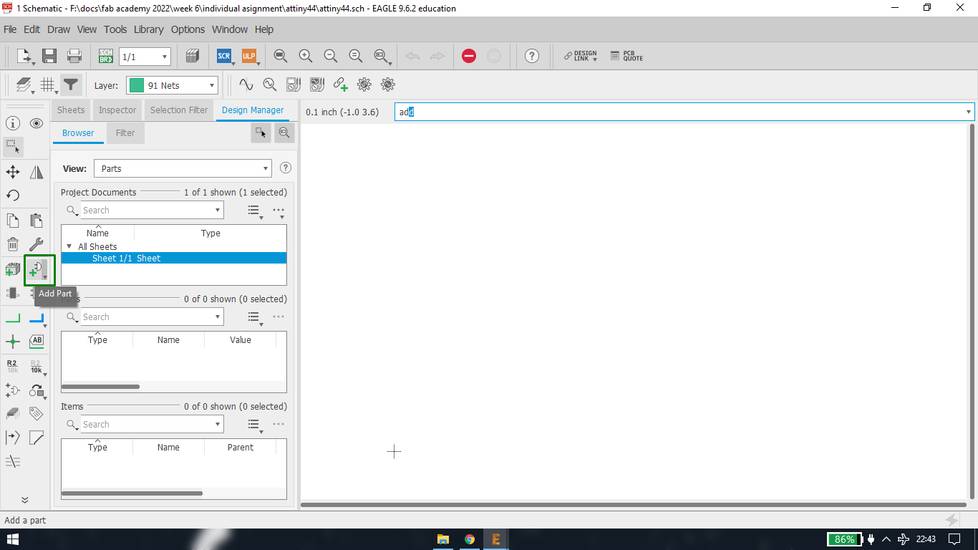
A window will pop up with the list of all the components,
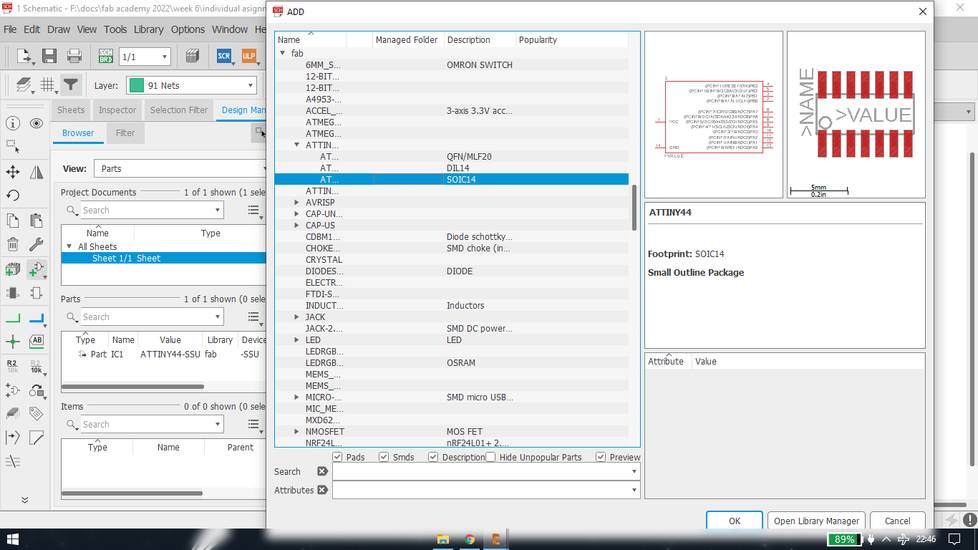
I highly recommend searching for the component manually because the “search” option inside the “add part” tab is very inaccurate. To add that
component into the schematic area, you can select the component and click on “OK” and you can also double click on the component. After that,
left click to drop the component into the schematic area, you can add the same components multiple times. If you just want one amount of the
selected component, hit escape key after dropping the component and you’ll be directed again to the “add part” tab and hit escape key twice to
exit the “add part” tab, which is a nice feature.
<<<---ADD LIBRARY--->>>
There are few components which can’t be found inside the pre-installed library so i had to install the fab library. You can download the fab
library from here : https://github.com/Academany/FabAcademany-Resources
1. You need to download the zip file. If you can’t see the green “code” button, click on the “pull requests” tab and again click on the
“<>code” tab and the green “code” button will appear, click on that and download the zip file.
2. Extract the zip file.
3. Open the library manager. You can open that by clicking on “library” > “open library manager”. You can also open the library manager by
clicking on “open library manager” from the “add part” tab
4. Inside the library manager, click on “available” tab
5. Inside the “available” tab click on “browse” button. Select the file type “EAGLE library” by going to the path where you have extracted the
zip file.
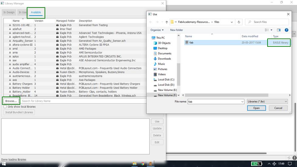
Now your library will be added and you can see the list of components inside the “add part” tab. Note that do not change the location of the
eagle library file from your system or else you’ll need to again add that library
<<<---CONNNECTING ALL THE COMPONENTS IN THE SCHEMATIC--->>>
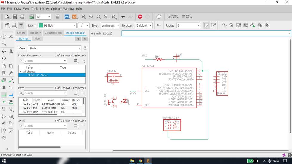
Once you have placed all the components, you need to give them the connection. You can do that with the help of “net” function. Just like
adding components, you can select the “net” function from the search as well as the button in the left panel.
You can always add more components and give them connection later. It is ot very difficult in the schematic, compared to routing in the
board.
You can connect the components in two ways,
1. Connecting the components through lines. Click on one end of the one component, drag the line however you want and click on the other
component. Doing this will make a connection between two components.
Now there might be a situation where there are a lot of components and in that case if you give connections using lines, it will be very
hard to interpret which component is connected to which component. So there is another way to set connection between two component
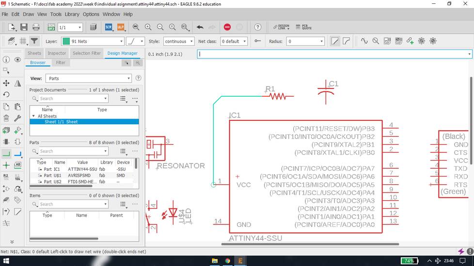
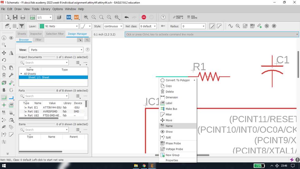
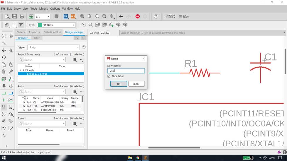
2. Connecting the components by assigning them names. Draw a small line using “net” function and assign that line a name by right clicking the
line and selecting “name”. In my case i wanted to connect the resistor to VCC so i gave “VCC” as name
Do the same with the vcc pin. If you’re asked for confirmation regarding the connection, click on yes
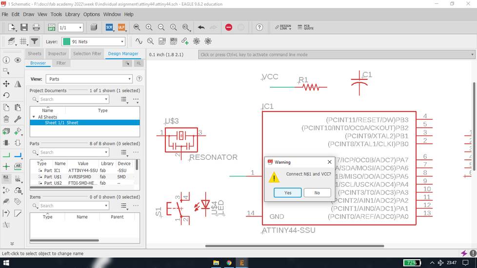
And your connection is made
It is always a good practice to assign the components names, it helps understand what components to solder on which pads. To assign the names
to the components, click on the “+” sign of the components and right clock and select “name”
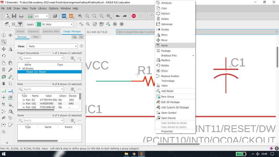
For every line or component, there will be a “+” sign, sometimes it will be very difficult to locate. So once you select any command like
“name”, “move“ or “rotate”, that command will be locked and now you don’t need to right click and select the command again and again for
every component. Once a particular command is locked, all you then need to do is click once in the “+” of other component and the selected
command will be applied to the other component. You can also select the command from the tools in the left panel.
<<<---ELECTRONIC RULE CHECK (ERC)--->>>
Once all the components are placed and connected in the schematic,
it is always recommended to check if there is any open circuit or if there is any junction not connected properly or if you forgot to add
value to the components. To do that there is a feature in eagle called Electronic Rule Check, you can find that in tools > ERC or
ctrl+shift+e
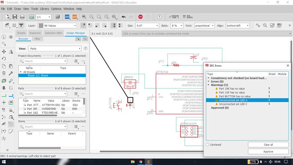
It will show you all the errors like component not connected or no value set for any component. You can check the errors and rectify them one
by one.
Connect the component

To add the value, double click on the name of component in the list under “parts” heading
There you can add/edit name and value. You won’t face any issue while routing the components inside board mode, however it is a good practice
to add the name as well as value because you’ll know that you have to place a resistor but you might forget what value resistor you are
suppose to place or if you don’t add a name, it will be difficult to know what component to place where just by looking at the pads.
<<<---DESIGN RULE CHECK (DRC)--->>>
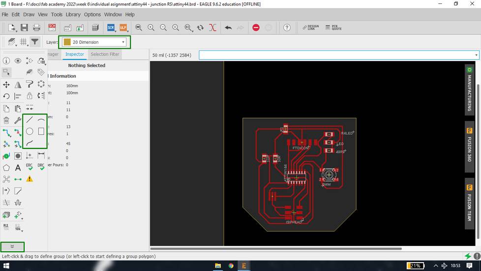
Just like the schematic mode, we can check if there is any error while routing the component. But unlike schematic, making even a tiny bit of
change can be very difficult, you’ll understand that in a minute. So before starting to route all the components, it is necessary to define
some parameters beforehand. We can do that with design rule check in board mode. To enter the board mode from schematic mode, click on the
“generate/switch to board” button on top or you can also search “board” in the search bar and you’ll be directed to the board mode. Inside
the board mode, all the components will be cluttered to the left side and with the move command you need to drag every component into the
canvas.
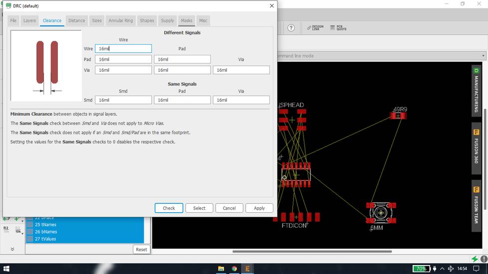
In the design rule check, I am just setting the parameter for the trace width and trace gap. To set that parameter i am referring to the PCB
we milled in group assignment in the electronics production week.
On the basis of that i set the clearance as 16 mil and maximum width(sizes) as 15 mil
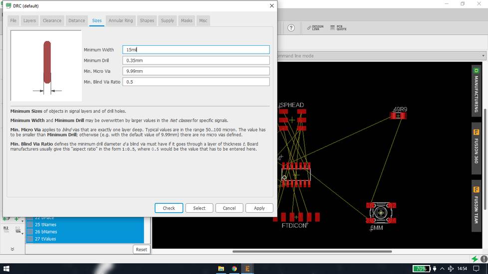
What this design rule check does,
1. It sets the trace width before you start routing, preventing you from any surprises later.
2. Sets the trace gap beforehand. With the move command, you can move the route and while doing that it will highlight red in between the traces
if the gap between the trace is less than the value set in the design rule check.
After the routing is is done, you can check for error by selecting tools > DRC or tools > errors, it will show you all kind of errors, if
there are any
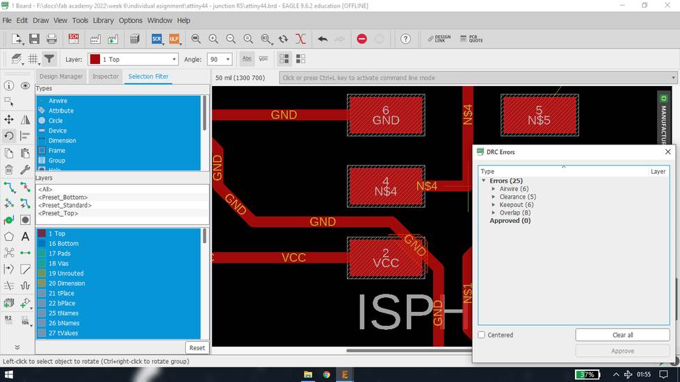
Check every error and try to rectify it.
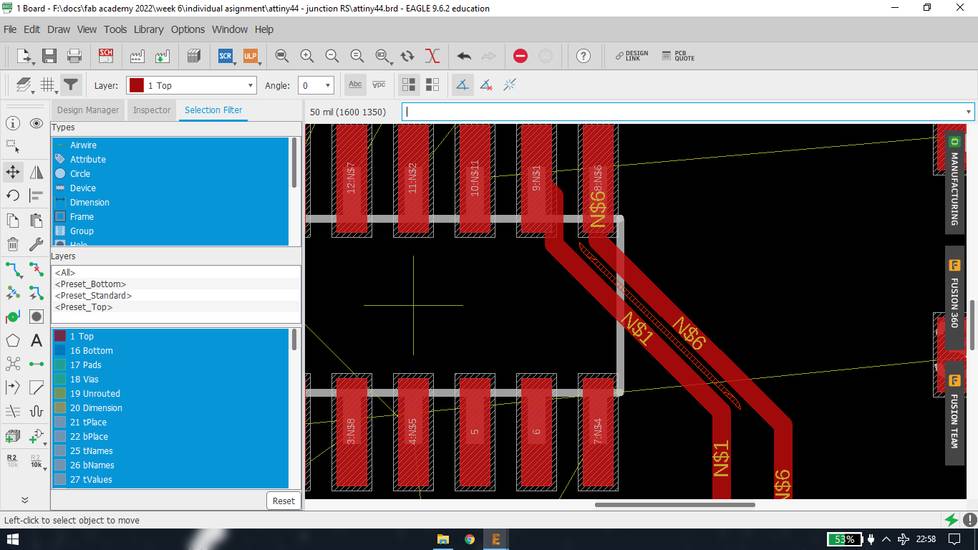
<<<---ROUTING--->>>
Routing means connecting two pads or making traces between two pads.
To route, select “route airwire” from the left panel or you can even search from the search bar on the top. To route, click on one side of
the pad and drag the line however you want and click on the other pad. Just follow the yellow reference line. It is always recommended to
select the 45° wire bend while routing. You can select that from the “select wire bend” button on the top
Note that when the route between two pads is complete, you will hear a sound of confirmation. If you didn’t hear the sound, that means the
route is not proper and you need to re-route. Also you can use multiple trace widths for routing. For example you can have all the traces with
16 mill size and for routing the trace between the pins or between the IC you can set the trace width/size to 10 mill just for that one
particular trace
Routing is just like playing the flow free game. For routing you can either move and rotate the components enough so that the yellow reference
line seems untangled enough and you can visualize the route before even starting or you can jump right into routing and figure out how you’ll
complete the route while doing it. I prefer the latter one.
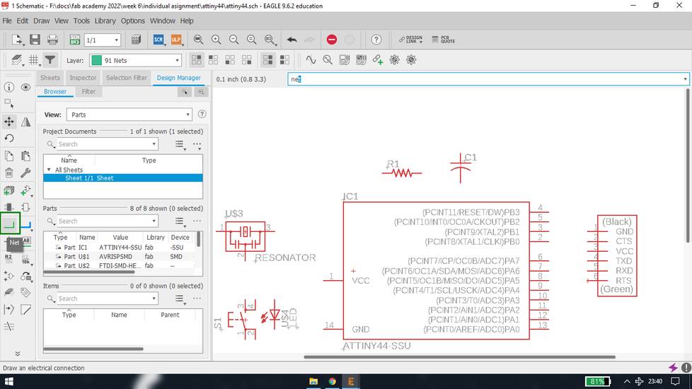
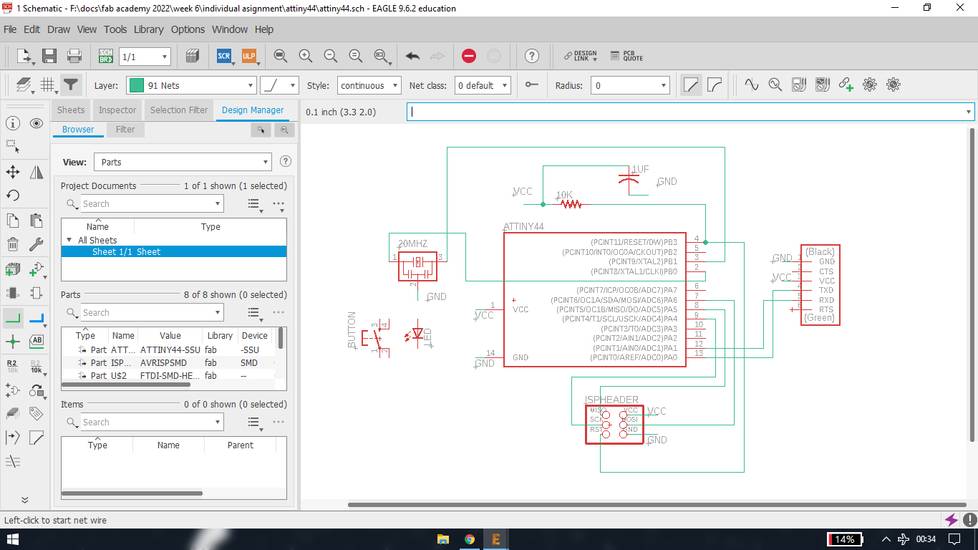
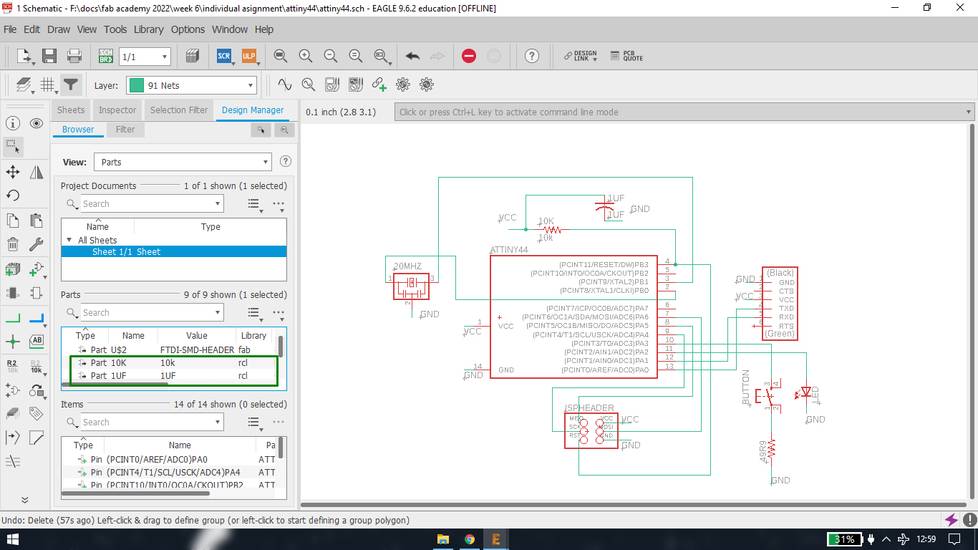
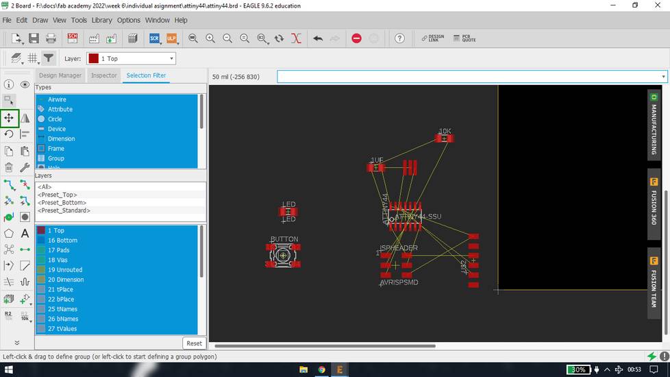
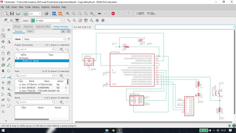
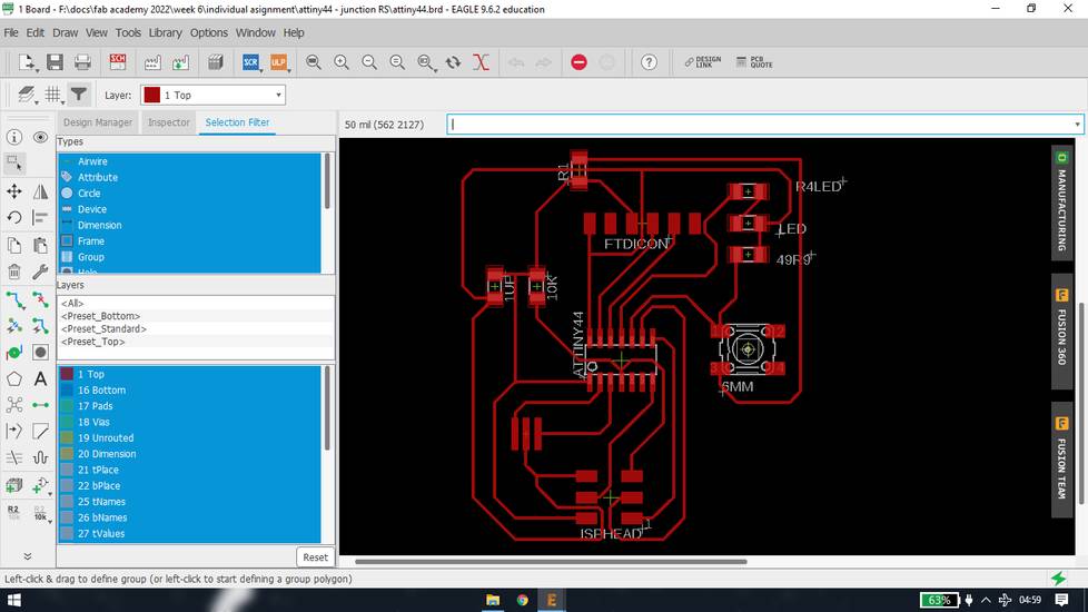
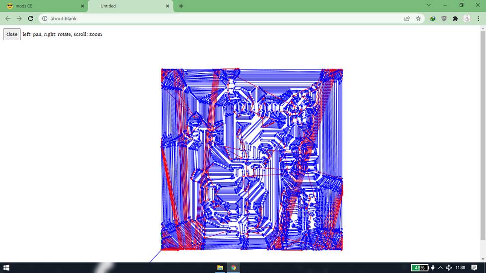
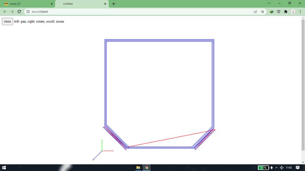
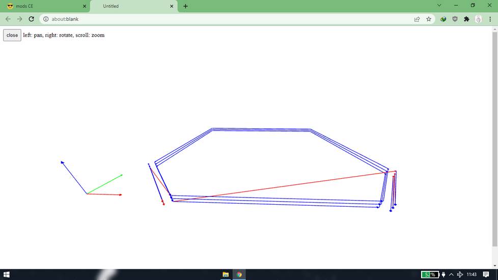
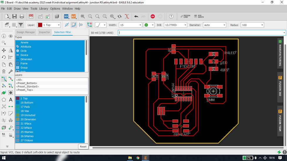
This was the schematic before i started routing,
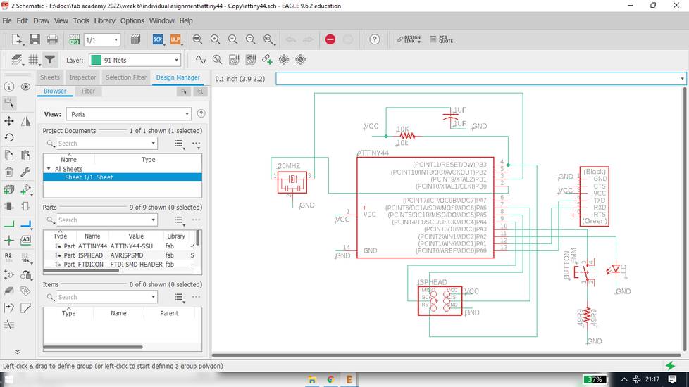
And this was the routing i did,

According to my local instructor, these are the mistakes i made with the schematic,
1. I did add a pull down resistor, however i forgot to add a resistor for the LED
2. The connection i gave for the button was similar to how i used to give for the digitalRead command in the arduino to read the state of the
button, back in the days when I was learning arduino.
This is the correct schematic according to my local instructor,
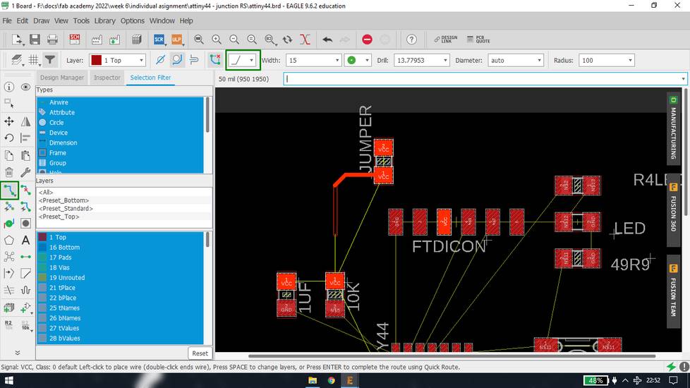
Since i added a component and change the connection of the button, i had to make the changes in the board. Connecting the new resistor for
led wasn’t very difficult, but connecting the button to the VCC of the IC was frustrating. This was the state of the board with just one loose
connection
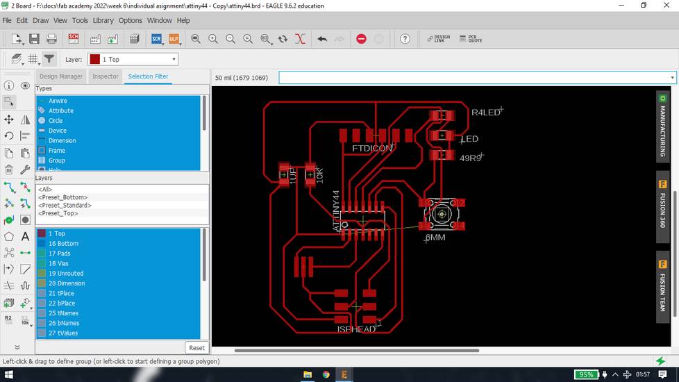
I tried to route without deleting the existing trace but that was not possible. So i deleted all the existing trace and tried to re-route the
whole board. After spending a few hours trying to re-route and getting no results, I then decided to use a 0 ohms resistor as a jumper. So
this is the final schematic and board (or i thought)
<<<---EXPORTING THE LAYOUT--->>>
You first need to draw the border of the pcb for cutting. So you’ll be exporting a trace file and an outline file. To draw the border, select
“dimension” beside “layer” on top. Click on the arrow in the bottom to expand the menu and with the shapes available there draw the border
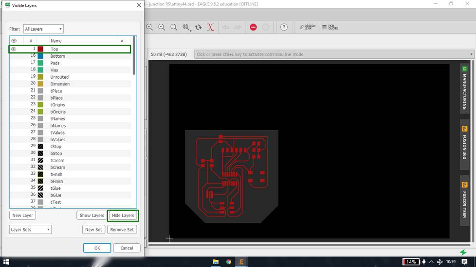
Delete the default square border. Now hide all the layers that you do not wish to export. To do that go to view > layer settings. Hide all the
layers by using “hide layers” button and click on the “eye” icon beside all the layer which you want to export. In my case i am exporting the
trace first so i am hiding all the layer except the top
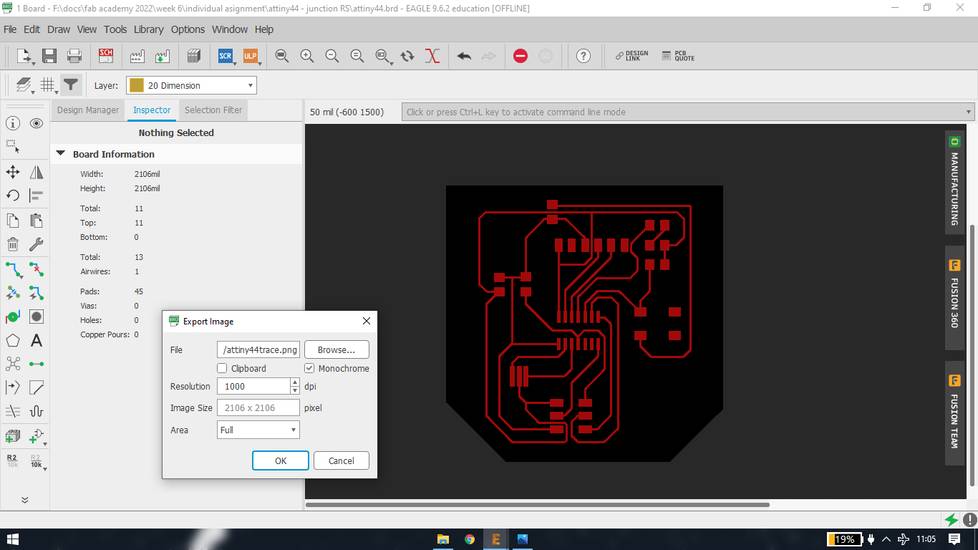
Go to file > export > image.
Check the monochrome option to export the image in black and white. Set the dpi to 1000 and after setting the export path, hit ok.
Do the same process with outline, however this time hide all the layers except the “dimension” one.
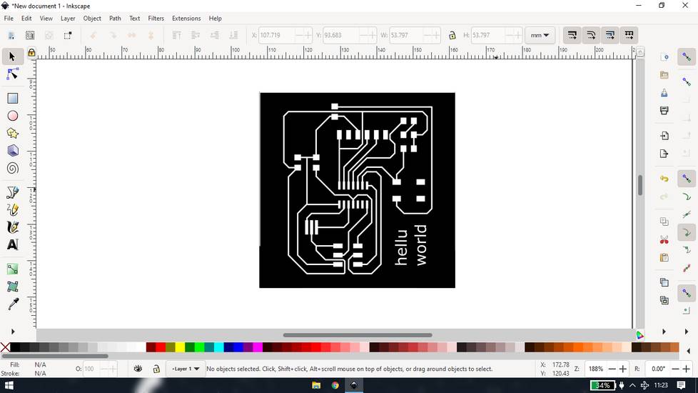
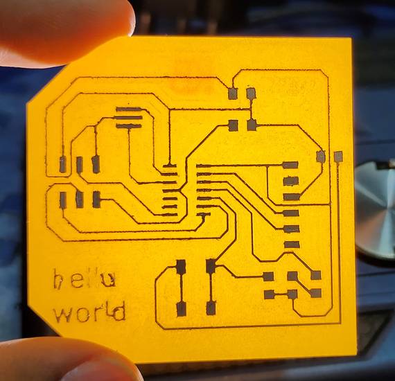
Because i didn’t realize that there is option to write text in the eagle itself, i edited the exported png file from inkscape
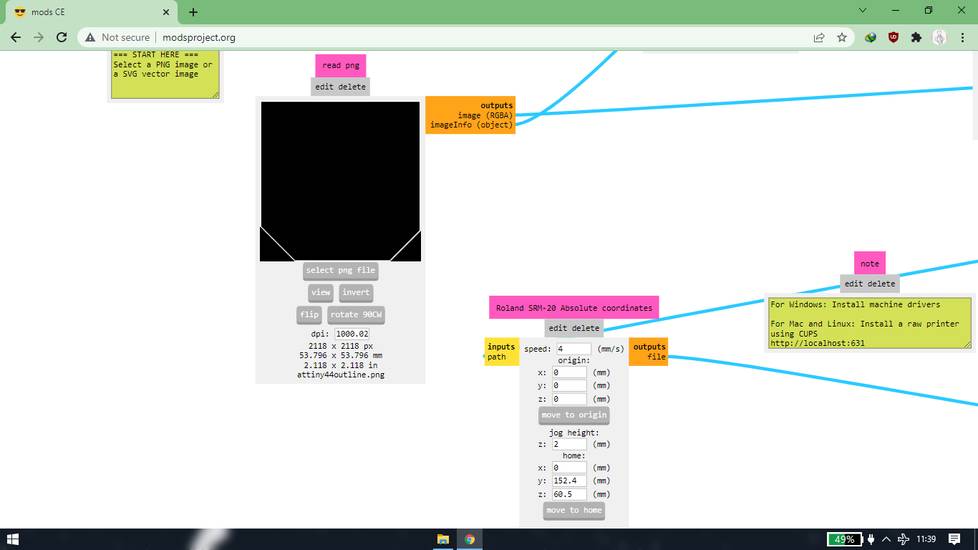
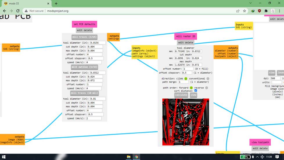
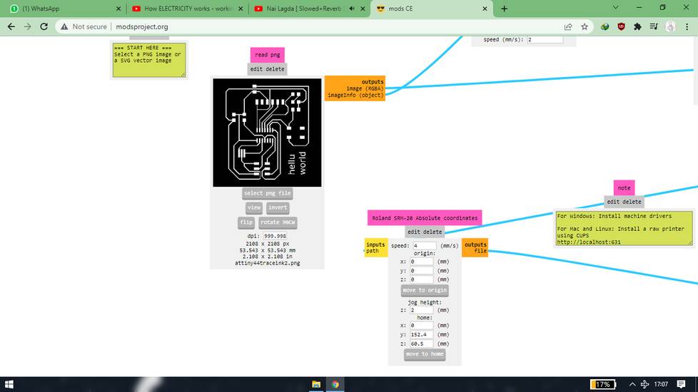
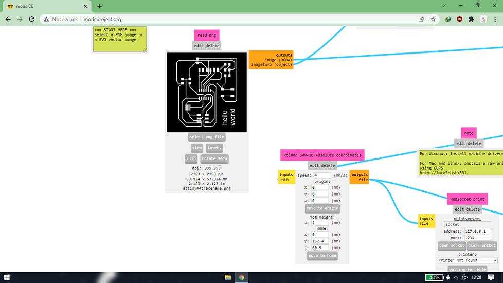
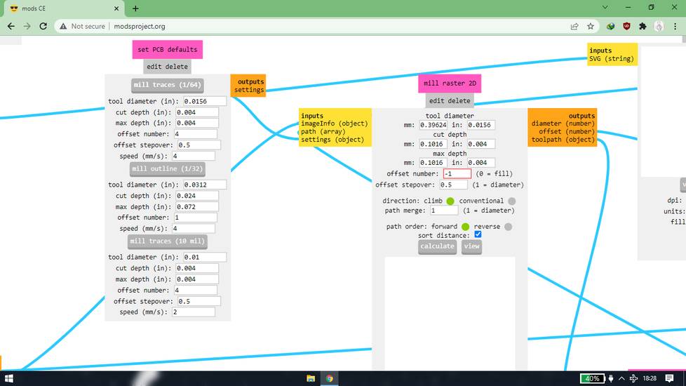
<<<---GENERATING THE TOOLPATH--->>>
trace
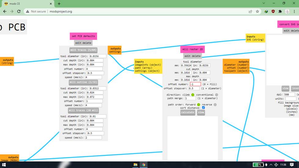
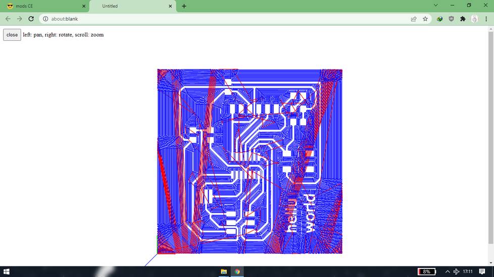
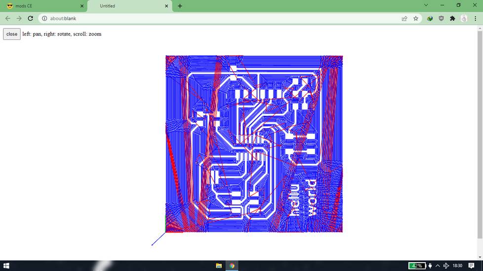
I used the mods community project to generate the toolpath. These are the settings i used for tracing,
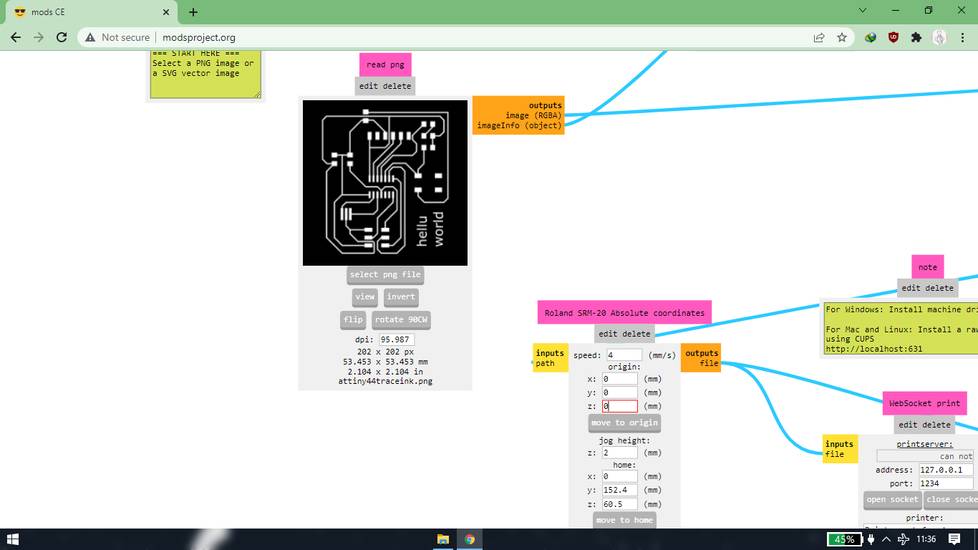
Since i was operating the SRM-20 with vpanel i just wanted to download the rml file so i deleted both the web socket print and web socket
device and connected the input file and output file
outline
Mistakes i made while designing and generating the toolpath
If you have observed, i made three mistakes while designing and generating the toolpath,
[1] Kept the default 96 DPI while exporting the file from inkscape.
[2] The mods community projects shows the dpi of the png image i selected, but i wasn’t paying attention.
[3] Didn’t make a connection inside the button in the schematic file. In the push button, the two pair of the pins are connected internally
which should be connected in the schematic as well, but it didn’t strike me eve after looking at the pads in the board mode
The rml file generated with 96 DPI and wrong button pads, i milled two PCBs
with vbit where the result was full of burr
with 1/64 endmill where the endmill broke
Mods settings was as given above
The rml file generated with 1000 dpi and wrong button pads, i milled 1 pcb
with same vbit where the vbit broke
Here are the mods settings
The last one i corrected the DPI as well as the button pads
with the same broken vbit
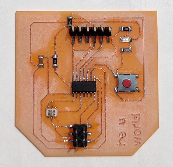
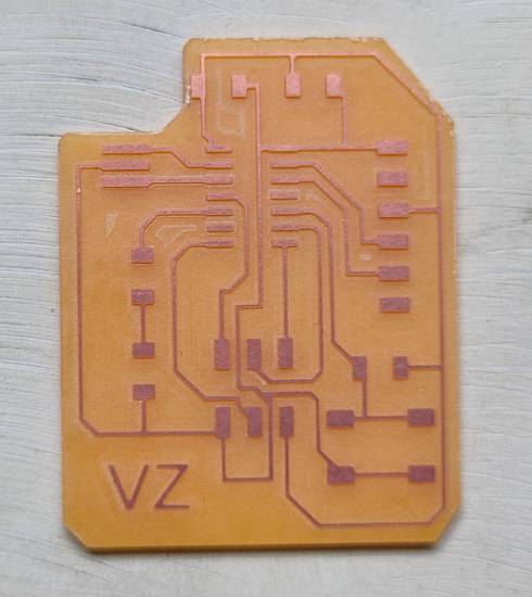
The final final schematic and board
And here are the mods settings
More of this in detail, later in milling part.
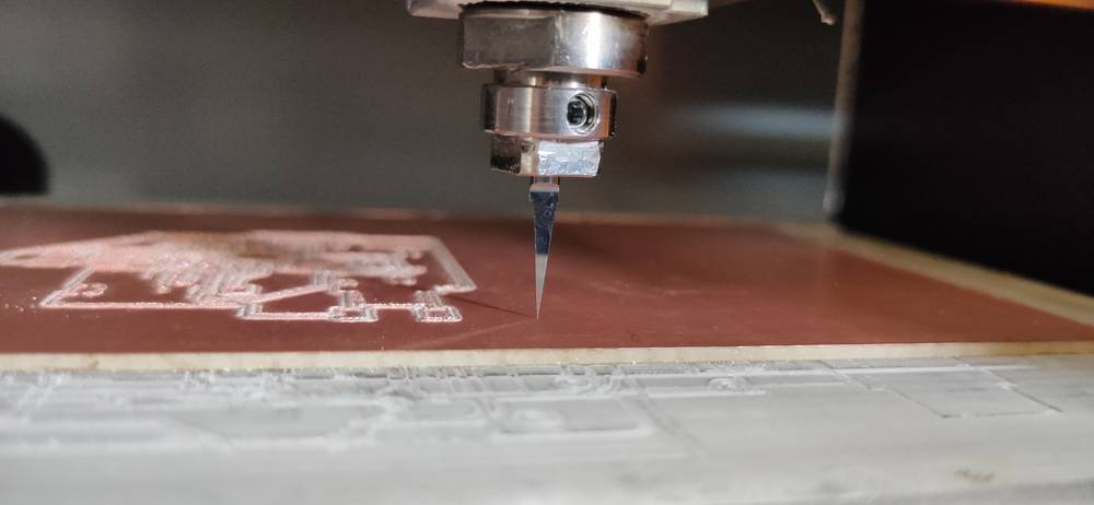
Milling
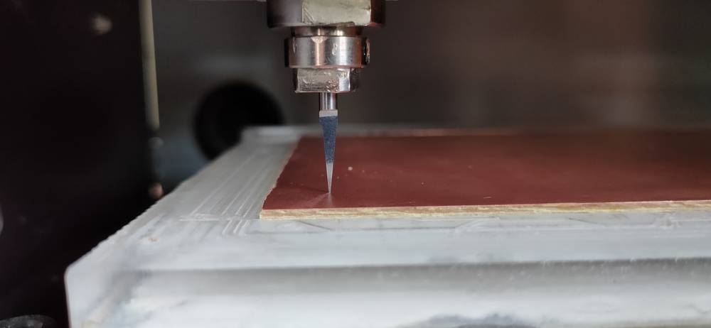
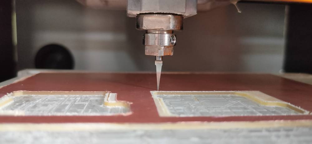
First i tried to mill the trace with the vbit,
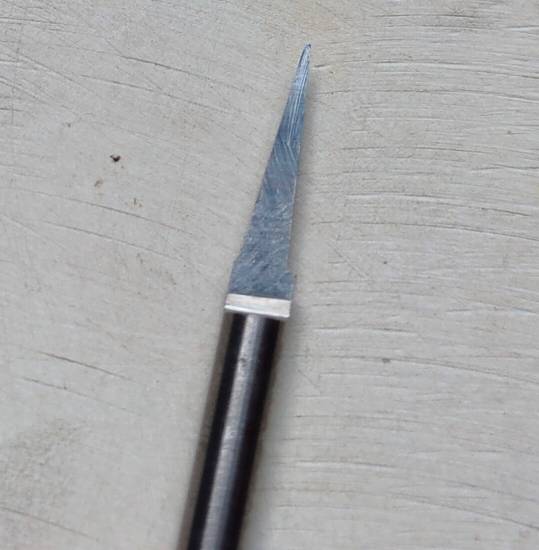
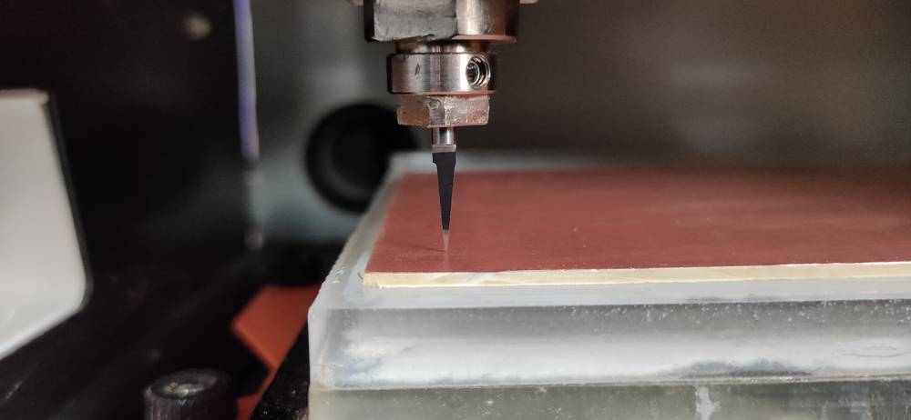
Position of vbit inside the chuck
Video of initial run,
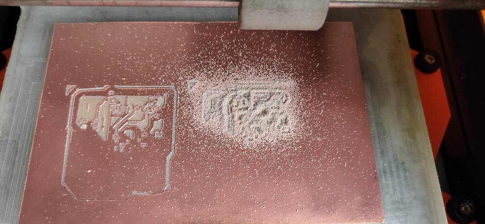
Outcome after few minutes, I paused to view the result. Since i saw the burr in the traces, i stopped the trace in the middle.
This was 96dpi
Then i tried the 1/64 endmill. Position of the endmill inside the chuck
Video of initial run
Video of endmill broken
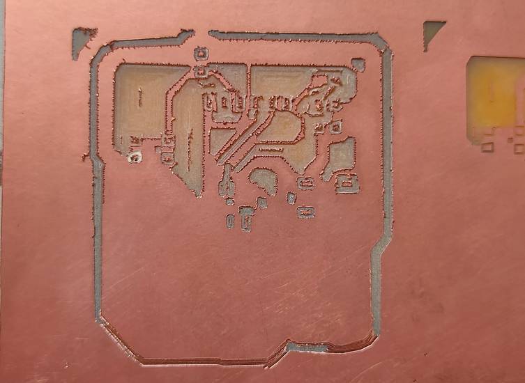
Trace after the endmill was broken. This was 96dpi
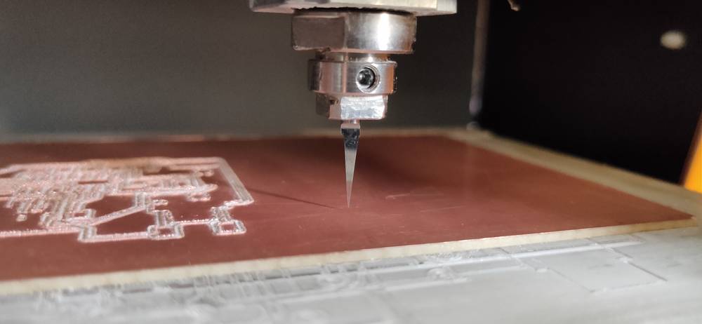
I then again tried with the vbit i used earlier. Position of the vbit inside the chuck
Video of the initial run
Video after the vbit was broken
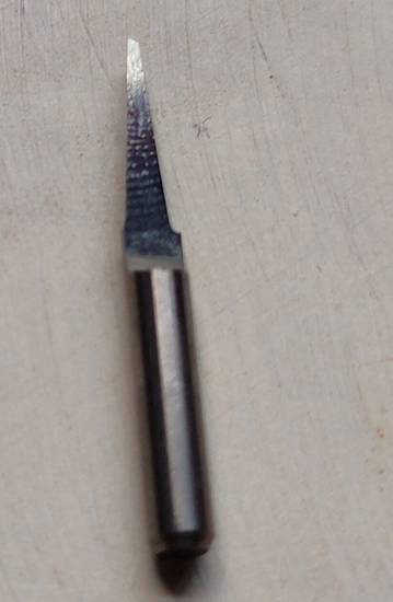
Image of broken vbit
Result of the trace after vbit was broken. This was 1000dpi
Bed leveling photos. I took this photos AFTER the vbit was broken though
Even though the vbit ws broken, i decided to continue the milling with the same broken vbit. I did the tracing from the beginning by doing the
zeroing process again.
Position of vbit inside the chuck,
After the trace
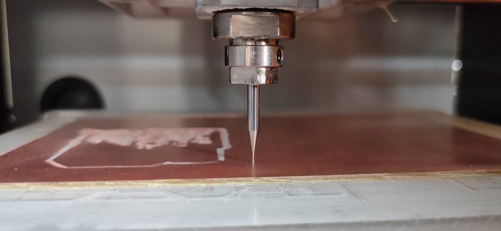
Cutting and position of 1/32 endmill. Position of endill inside the chuck
After cutting
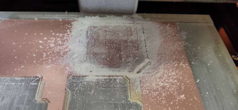
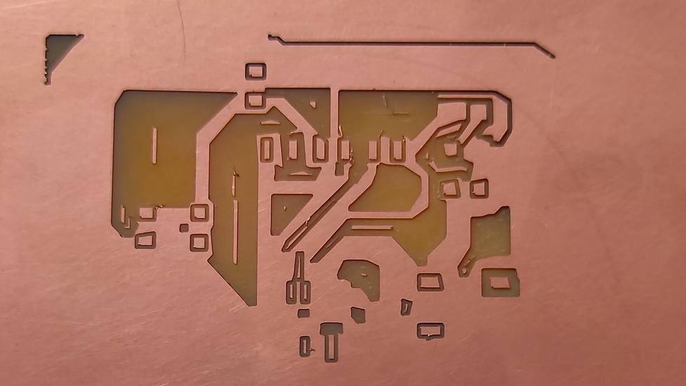
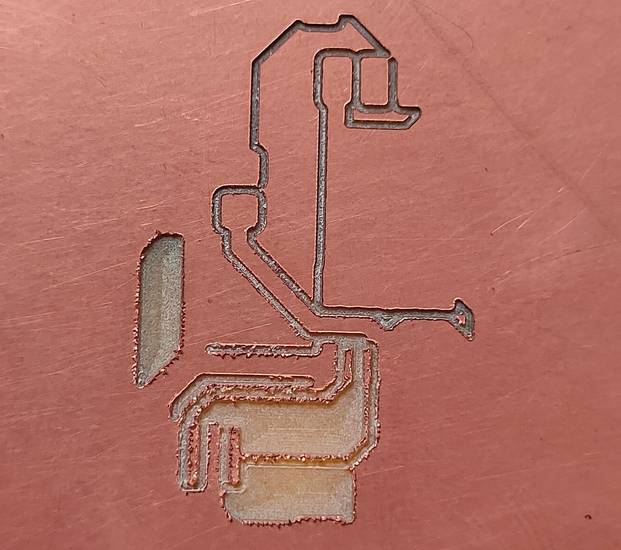
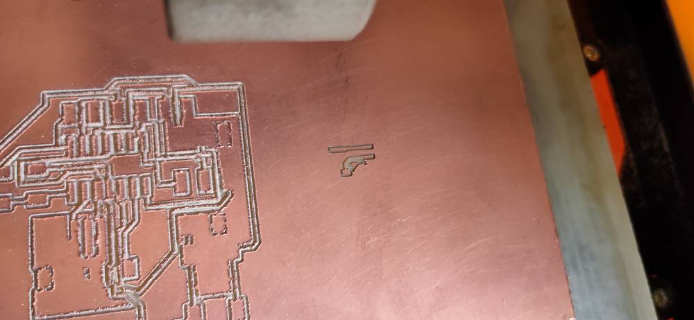
here are the results of the trace with the broken vbit,
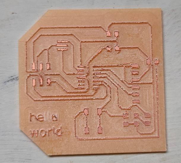
The finishing of the trace was very rough. It took a lot of time to remove the burr from the pads. I cleaned the border just enough so that
the components can be easily placed in the pads
I did check the pcb with the continuity function in multimeter and there were no open circuit between the traces and pads, so i proceeded with
the soldering
Soldering
Here is the list of components required,
2*3 SMD male header pins
1*6 SMD male header pins
Attiny44 IC
Push button
LED
10K ohms resistor
100 ohms resistor
49.9 ohms resistor
0 ohms resistor
1 UF capacitor
20 MHZ resonator
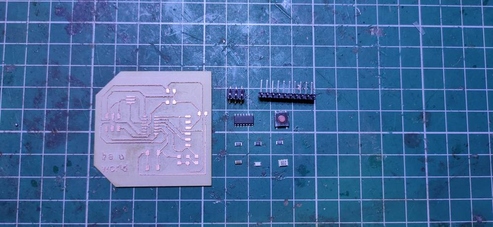
(i forgot the 10k ohms resistor)
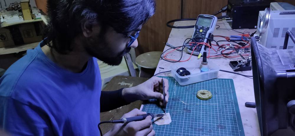
Even after removing the burr from the border of the pads, i did face some issue while soldering the components. Because of the burr, the
components were not placing flatly onto the pad, it was behaving like a seesaw when placed onto the pads. I still managed to solder the
components onto the PCB. Except for the fdti header pin that was soldered slantly, everything seemed fine.
Our instructor told us to find out the reason behind breaking off all the bits. We explained what all we did while milling and showed the
outcomes of the traces in the PCB.
Our instructor decided to try millig the PCB himself. Just like we did with generating the rml file, he didn’t change anything in the mods
community project except for setting the absolute coordinates to zero.
Position of the vbit inside the chuck
After setting the XY and Z coordinates as the origin and before giving the output command, the endmill was positioned a bit above the bed
so that when we hit the output command, the spindle would gain the 9000 rpm speed in the air and not while the tip of vbit is touched to the
PCB. After giving the output command and the spindle gained the speed of 9000 rpm, the tip of the vbit broke the movement it touched the PCB
to start the trace. We concluded that the tip of the vbit broke when the vbit was milling in the air,
Photo of the broken vbit
(the damage is very minor, i can’t even see that in the image captured.)
Our instructor took another bit to test it again with the same settings as before. This time the vbit traced for about a minute or so when the
vbit started milling in the air and we concluded that the bit was broken yet again.
outcome of the trace
Seeing the trace, it looked like the vbit was engraving very deep. So instead of using the settings of 1/64 endmill from the mods community
project which is 0.1016 mm cut depth and 0.1016 mm max depth we changed it to 0.0800 as cut depth and max depth, and this time we used the
same old vbit that was just broken,
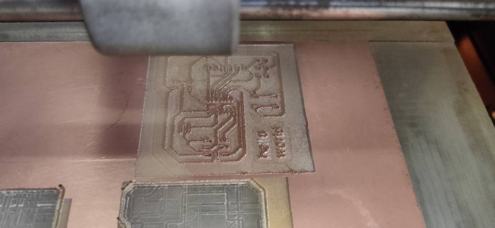
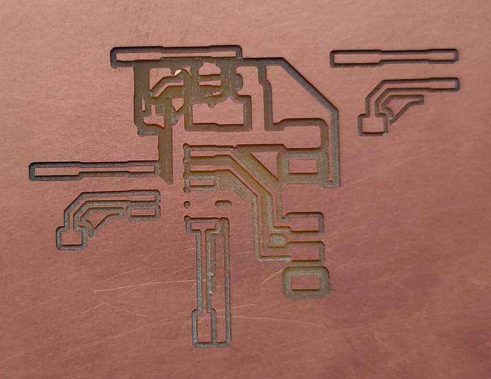
This is the result of the trace,
The trace was very clean but because of some mistake in design, we stopped the print in the middle and milled a new pcb with different design
and same broken vbit and same settings of 0.0800 mm cut depth and max depth. This was the result after the trace,
The traces came out better than the 1/64 endmill.
Some conclusions according to me:
In the electronics predictions week, i milled the fabISP with the 1/64 endmill which was assigned to each student. At that time i had no issue
with the milling, like no burr in the trace or no breaking of the endmill. Everything with milling went well in the first try
In the same week of electronics production, i milled the JTAG pcb with the vbit. For the toolpath, i used the same setting i use for 1/64
endmill. You can see the outcome in the tab for electronics production. At that time i got great results with the vbit for the tracing part,
like there were no major burr on the pads or traces and also the vbit didn’t break. Faced no issue while soldering too.
In the week of electronics production, before i had milled my PCB, few of my colleagues had already broken their endmills. Our instructor
assumed that the reason behind the breaking of endmill was that the endmill was too much outside the chuck so what happens is that at 9000
rpm, the endmill starts to wobble and hence result into breaking the tip of endmill. So when our instructor set the endmill inside the chuck
for me, i clicked the photo of that and inserted the same amount of endmill inside the chuck this time as our instructor had done before, by
referring to the photo. So positioning of the endmill inside the chuck is not the issue. This week, i checked the bed level AFTER the endmill
was broken and it was fine, so bed level is not an issue either. Before starting the milling, i did check if the copper clad was warped, and
it was fine. After sticking the copper clad onto the bed, i pressed the copper clad firmly onto the bed to remove any bubbles at the bottom of
the copper clad, so the copper clad is also fine(we are using the FR1 copper clad). The speed of the spindle rotating is always around
9000-9600 rpm. The speed of tracing is always 4mm/s. Apart from setting the absolute coordinates to 0 for XYZ and changing the offset to -1,
I am keeping all the settings as it is while generating the toolpath with mods community project.. To operate the SRM-20, i am using the
Vpanel.
I am not able to conclude why my 1/64 endmill broke or why everyone’s(literally) 1/64 endmill broke.
Talking about the vbit, i set the same amount of vbit inside the chuck as i did the last time. Used the same toolpath settings which i had
used earlier which is use the settings for 1/64 endmill and use vbit instead, and yet every single vbit we used this week, broke.
There are 2 cases,
- Using the vbit which is already broken
If you have read the description above, when i used the broken vbit to mill, my pcb came out to be full of burr. When my colleague used
another broken vbit, the result was even better than the 1/64 endmill. I guess the outcome of the trace is dependent on how much chunk of the
vbit is broken. Even after concluding that using the 0.0800 cut depth and max depth will give better result after we milled my colleague’s
pcb with broken vbit, when my other colleague milled the pcb with same broken vbit and same settings, it again came out full of burr. So i
still don’t know if i will get the pcb full of burr or clean like we get earlier by using the broken vbit
- Using the fresh vbit
Well, every vbit we used broke at one point or another. In some cases very tiny chunk of vbit was broken and in some cases comparatively large chunk of piece was broken. So i guess the tip of the vbit is bound to be broken, all we need to take care is that a very tiny amount of the tip gets broken. So we had concluded that in the new vbit, use cut depth and max depth as 0.0700 and after one pass of the endmill see it the endmill gets broken. If not broken, see the outcome of the trace. If the trace is not properly cut because of 0.0700 cut depth, without changing the origin of XYZ, give the second pass with 0.0800 and see the result.
If the vbit do get broke do the zeroing process and with the 0.0800 cut depth and max depth, start milling the trace again and see if the pcb comes out clean or full of burr.
In a nutshell, i still don’t know for sure what are the best setting to use in order to get best results from the vbit.
Programming
In the electronics production week, i had made fabISP which is a programmer. In this week of electronics design, i made a hello world board.
To check whether the hello world board i made actually works or not, i had to program it. To program the hello world board you need a
programmer, which is the fabISP.
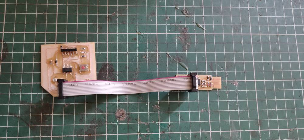
You need to connect both the PCB with a IDC connector and a ribbon cable. Make sure that the alignment of
MISO VCC
SCK MOSI
RST GND
of the fabISP and the hello world board is proper. What i mean is that the MISO pin of the fabISP should be connected with the MISO pin of
hello world, GND pin of the fabISP should be connected with the GND pin of the hello world board and so on.
In my case this is the proper alignment
In the electronics production week, i made the fabISP a programmer by connecting the fabISP to a programmer via IDC connector and a ribbon
cable and connecting the programmer to the pc via USB extension cable. Using the same principle i had to program my hello world board. This
time i already have my programmer and i am just programming another board with the programmer and not making another board a programmer.
Connect the hello world board to the fabISP via IDC connector and ribbon cable and connect the fabISP ot the pc via USB extension cable
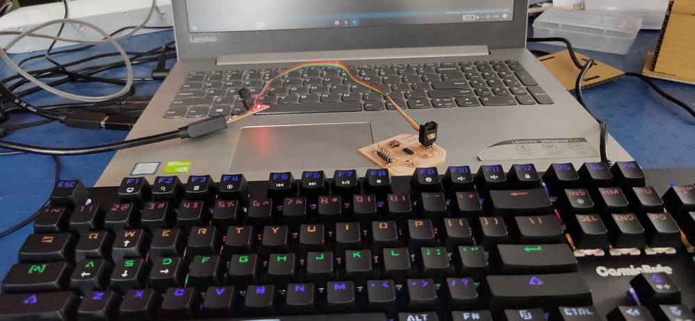
For programming the hello world board, i am using Arduino IDE.
Link for downloading/installing Arduino IDE: https://www.arduino.cc/en/software
You need to setup a few things before uploading the program to the hellp world board via fabISP.
[1] Add/Change Additional Boards Manager URL to: http://drazzy.com/package_drazzy.com_index.json
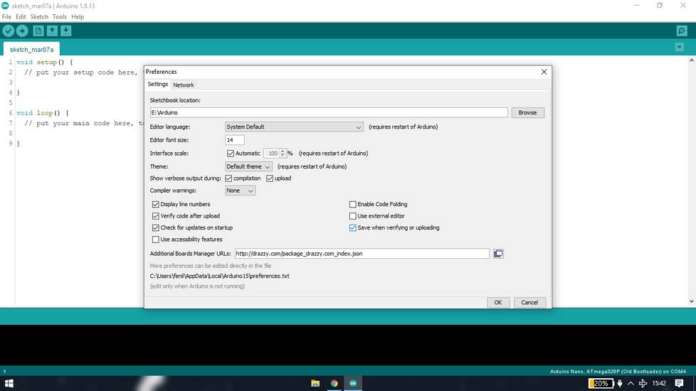
Go to file > preferences and in the Additional Boards Manager URL paste the above link
[2] Install ATTinyCore board by Spence Konde
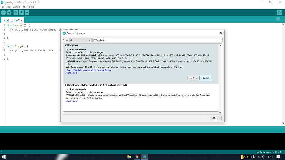
Go to tools > board > board manager and search for ATTinyCore and install the one by Spence Konde
[3] Select the following things in the tools
- Go to tools > board > ATTinyCore and select ATTiny 24/44/84(a) (no bootloader)
- Go to tools > chip and select Attiny44(a)
- Go to tools > programmer: and select USBTinyISP (ATTinyCore) SLOW, for new or 1MHZ parts
Your tools menu should look like this after selecting all the things
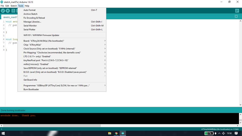
Go to tools and select burn bootloader and it should show message like “Done burning bootloader”. Fortunately i was able to burn the
bootloader on the second try because on the first try i forgot to select the programmer from the tool menu.
My colleague was getting the “error while burning bootloader” message on the first try too. He had downloaded the zip file from the Arduino
website and extracted the folder so I suggested installing the software rather than using the downloaded folder. He tried that and was able
to successfully burn the bootloader and upload the program too.
So apart from looking in the tool menu to see if all the necessary options are selected and check if the Arduino software you are using is
installed and not extracted, i don’t know what to do if you are unable to burn the bootloader.
<<<---BLINKING--->>>
I first tried the blink code to check if the LED works. You can get the code by going to file > examples > basics and select blink. Prefer to
the schematic of your hello world board and set the led pin number accordingly
You can copy the code from here,
you can copy the code from here too.
<<<---BUTTON AND LED--->>>
The i tried the code i had written few years ago when i was learning Arduino, i changed the led and button pin according to the schematic of
my hello world board
You can copy the code from here,
you can copy the code from here too.
<<<---BUTTON AND LED 2--->>>
Compared to my colleagues, the brightness of my led was too low. So tried the code they were using. To get that code go to file > examples >
digital and select button. Assign the led pin and button pin according to the schematic
You can copy the code from here,
you can copy the code from here too.
Group assignment
group assignment link
https://fabacademy.org/2022/labs/vigyanashram/groupassig/groupassignment4.html
You can download the hello world board and schematic file from here:
hello world
Drip Irritation by Fenil Chandarana is licensed under Attribution-NonCommercial-NoDerivatives 4.0 International![]()
![]()
![]()
![]()